
Samsung's 12-High HBM4 Stack Pushes Memory to 128GB Per Package
Samsung's next HBM generation targets a fourfold-plus capacity jump over today's frontier accelerator configs — and it's co-designing the spec directly with GPU vendors for a 2027 production window.
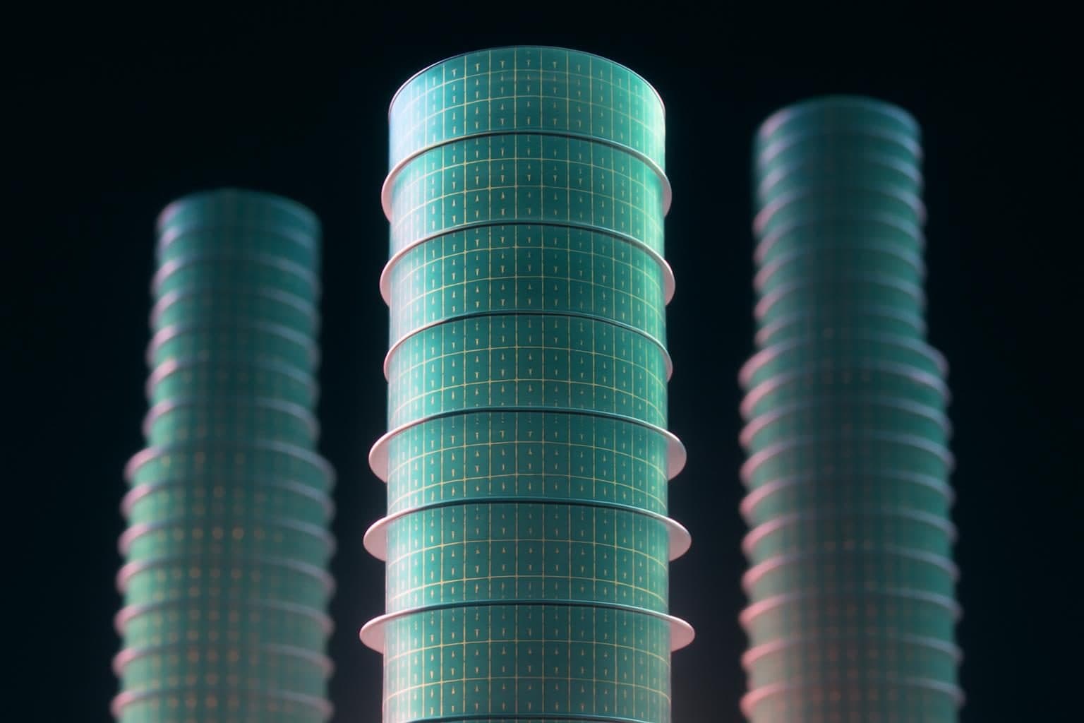
The memory bottleneck in AI infrastructure is about to get a serious intervention. Samsung Electronics has disclosed plans for an HBM4 package built on a 12-high stacked DRAM die architecture, targeting up to 128GB per package — a figure that dwarfs the 24–32GB HBM3E configurations currently shipping inside the industry's frontier AI accelerators.
This isn't a roadmap slide. Samsung says it is already co-developing HBM4 with major GPU vendors and has set mass production for 2027, timed explicitly to align with next-wave AI accelerator programs.
Why the Capacity Jump Matters Now
The driver isn't incremental model scaling — it's the structural demand of multi-trillion-parameter training runs and the push toward dramatically larger context windows. Samsung executives named frontier model training as the primary use case, and the numbers bear out why memory capacity, not just bandwidth, has become the constraint.
A package ceiling of 24–32GB forces GPU designers to tile more HBM stacks onto a substrate, multiplying interposer area, power draw, and yield complexity. A single 128GB HBM4 package changes that calculus: fewer stacks can support the same working-set size, or the same stack count can hold dramatically more model state on-chip. Either path compresses the frequency and cost of traffic to slower off-package DRAM tiers.
The Engineering Bets Behind the Stack
Getting to 12 dies high isn't purely a die-count exercise. Samsung acknowledged that advanced 3D packaging and new thermal management techniques are required to sustain higher bandwidth without breaching the power envelopes that data center operators enforce at the rack level. Heat is the physics problem that multiplies with every added layer — dissipating it through a stack that is, by definition, designed to minimize lateral footprint demands new thermal pathways rather than bigger heatsinks.
Underpinning the whole architecture is continued investment in next-generation TSV (through-silicon via) and interposer technologies. TSVs are the vertical copper conductors that carry data between stacked dies; at 12 high, the aspect ratios, fill uniformity, and stress management all become harder. Interposer design — the silicon or organic substrate that connects HBM to the GPU die — must simultaneously handle higher pin counts, tighter pitch, and the thermal load the stack generates. Samsung's bet is that its process capabilities in both areas can be production-ready on the 2027 timeline.
Co-Development as a Competitive Signal
The detail worth tracking is the co-development structure. Samsung isn't announcing a spec and waiting for customers — it is building HBM4 in active partnership with the GPU vendors whose accelerator roadmaps will absorb the product. That approach shortens the integration risk on both sides: the memory stack and the compute die can be tuned against each other before either reaches production masks.
It also signals where the competitive pressure is coming from. SK Hynix supplied HBM3E to the leading AI accelerator programs at volume before Samsung and Micron reached comparable yields. Co-developing HBM4 with GPU vendors is a direct attempt to close that design-in lead — locking in socket wins at the architecture stage rather than competing purely on yield and pricing at qualification.
The Bigger Shift
What Samsung's HBM4 disclosure actually marks is the maturation of memory as a first-class AI infrastructure variable — no longer a component that GPU designers spec after the compute architecture is fixed, but a co-designed subsystem that shapes what models can be trained and inferred at all. When a memory package goes from 32GB to 128GB, the ceiling on what fits in a single accelerator's working memory moves, and with it, the viable design space for next-generation AI systems. The 2027 production target gives the industry a concrete horizon to plan against. Whether Samsung holds that timeline — and whether it does so ahead of its competitors — will determine which accelerator generation it actually powers.